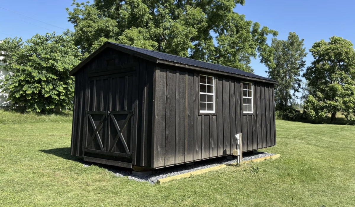
Setting up a semiconductor-grade cleanroom is often regarded as a complex and costly venture reserved for large corporations. However, innovative enthusiasts have demonstrated that it is possible to create a functional cleanroom environment within a modest wooden shed, enabling basic chip manufacturing processes at home.
The Concept Behind a DIY Cleanroom
Cleanrooms are controlled environments designed to eliminate dust, airborne microbes, and chemical vapors that can compromise semiconductor fabrication. Typically, they require advanced air filtration systems, carefully managed pressure differentials, and strict protocols. The DIY approach adapts these principles into a more accessible form.
By constructing an enclosure in a wooden shed and employing high-efficiency particulate air (HEPA) filters along with ventilation fans, makers can reduce contamination to acceptable levels. This allows some experiments and prototyping in chip production without access to commercial facilities, albeit at a simpler scale.
Key Design Elements and Equipment
The first step involves sealing the interior space to prevent uncontrolled airflow and introducing filtered air via HEPA systems. Maintaining positive air pressure inside the cleanroom helps keep contaminants out.
Temperature and humidity control are also important to ensure process stability. Makers often repurpose consumer-grade equipment combined with precise monitoring instruments to achieve this balance, adapting to budgetary and technical constraints.
Challenges in DIY Semiconductor Fabrication
While building the cleanroom is achievable with dedication, the subsequent steps of semiconductor manufacturing require intricate photolithography, deposition, and etching processes that are highly sensitive and equipment-intensive.
Handling hazardous chemicals and nanoscale precision are significant obstacles. Therefore, the chips produced by home setups are typically rudimentary or demonstrative rather than fully functional integrated circuits found in commercial electronics.
Potential Applications and Educational Value
Despite limitations, such DIY cleanrooms serve crucial roles for educational purposes, hobbyist experimentation, and proof-of-concept demonstrations. They help demystify semiconductor technology and inspire innovation beyond traditional institutional boundaries.
Moreover, this movement encourages open-source hardware development and could foster new communities focused on low-cost semiconductor experimentation and learning.
Future Prospects in Homegrown Semiconductor Manufacturing
Advancements in materials science, miniature fabrication equipment, and automation may eventually lower barriers further, enabling more sophisticated chip production outside industrial settings.
Continued interest and experimentation in this domain could expand access to semiconductor technologies and stimulate grassroots innovation in electronics design and fabrication.